The fact that the metallic elements are found on the left side of the periodic table offers an important clue to the nature of how they bond together to form solids.
- These elements all possess low electronegativities and readily form positive ions Mn+. Because they show no tendency to form negative ions, the kind of bonding present in ionic solids can immediately be ruled out.
- The metallic elements have empty or nearly-empty outer p-orbitals, so there are never enough outer-shell electrons to place an octet around an atom.
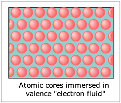 These points lead us to the simplest picture of metals, which regards them as a lattice of positive ions immersed in a “sea of electrons” which can freely migrate throughout the solid. In effect the electropositive nature of the metallic atoms allows their valence electrons to exist as a mobile fluid which can be displaced by an applied electric field, hence giving rise to their high electrical conductivities. Because each ion is surrounded by the electron fluid in all directions, the bonding has no directional properties; this accounts for the high malleability and ductility of metals.
This view is an oversimplification that fails to explain metals in a quantitative way, nor can it account for the differences in the properties of individual metals. A more detailed treatment, known as the bond theory of metals, applies the idea of resonance hybrids to metallic lattices. In the case of an alkali metal, for example, this would involve a large number of hybrid structures in which a given Na atom shares its electron with its various neighbors.
 The most useful treatment of metallic solids is based on the molecular orbital approach.
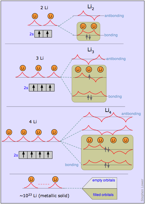
It is best understood by considering first a succession of molecules based on lithium (or any other alkali metal having a single s electron in its valence shell). The figure below shows how the MO wave functions for Li2, Li3 and Li4 will look. These are all constructed by combining the individual atomic s functions just as is done in simple MO theory. The only thing new here is that the new molecular orbitals extend over all the atoms of the metal, and that the orbitals of intermediate energy possess both bonding and antibonding character in different regions. Every time we add another atom, we get two new MO’s, but since each atom contributes only a single valence electron, the MO’s are never more than half filled. If we extrapolate this to a giant “molecule” LiN containing a very large number of atoms, we get 2N MO’s that are so closely spaced in energy that they form what is known as a band of allowed energies. In metallic lithium only the lower half of this band is occupied.
Metallic solids possess special properties that set them apart from other classes of solids and make them easy to identify and familiar to everyone. All of these properties derive from the liberation of the valence electrons from the control of individual atoms, allowing them to behave as a highly mobile fluid that fills the entire crystal lattice. What were previously valence-shell orbitals of individual atoms become split into huge numbers of closely-spaced levels known as bands that extend throughout the crystal.
Why metals have high strengths and high melting points
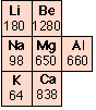 The strength of a metal derives from the electrostatic attraction between the lattice of positive ions and the fluid of valence electrons in which they are immersed. The larger the nuclear charge (atomic number) of the atomic kernel and the smaller its size, the greater this attraction. As with many other periodic properties, these work in opposite ways, as is seen by comparing the melting points of some of the Group 1-3 metals (right). Other factors, particularly the lattice geometry are also important, so exceptions such as is seen in Mg are not surprising.
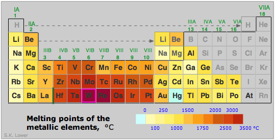 In general, the transition metals with their valence-level d electrons are stronger and have higher melting points: Fe, 1539°C; Re 3180, Os 2727; W 3380°C.
(W is tungsten, the highest-melting metal of all; do you know what principal use derives from this very high melting point?)
Why metals are malleable and ductile
 These terms refer respectively to how readily a solid can be shaped by pressure (forging, hammering, rolling into a sheet) and by being drawn out into a wire. Metallic solids are known and valued for these qualities, which derive from the non-directional nature of the attractions between the kernel atoms and the electron fluid. The bonding within ionic or covalent solids may be stronger, but it is also directional, making these solids subject to fracture (brittle) when struck with a hammer, for example. A metal, by contrast, is more likely to be simply deformed or dented.
Why metals are good electrical conductors

In order for a substance to conduct electricity, it must contain charged particles (charge carriers) that are sufficiently mobile to move in response to an applied electric field. In the case of ionic solutions and melts, the ions themselves serve this function. (Ionic solids contain the same charge carriers, but because they are fixed in place, these solids are insulators.) In metals the charge carriers are the electrons, and because they move freely through the lattice, metals are highly conductive. The very low mass and inertia of the electrons allows them to conduct high-frequency alternating currents, something that electrolytic solutions are incapable of. In terms of the band structure, application of an external field simply raises some of the electrons to previously unoccupied levels which possess greater momentum.
The conductivity of an electrolytic solution decreases as the temperature falls due to the decrease in viscosity which inhibits ionic mobility. The mobility of the electron fluid in metals is practically unaffected by temperature, but metals do suffer a slight conductivity decrease (opposite to ionic solutions) as the temperature rises; this happens because the more vigorous thermal motions of the kernel ions disrupts the uniform lattice structure that is required for free motion of the electrons within the crystal. Silver is the most conductive metal, followed by copper, gold, and aluminum.
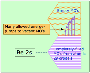 Metals conduct electricity readily because of the essentially infinite supply of higher-energy empty MOs that electrons can populate as they acquire higher kinetic energies. This diagram illustrates the overlapping band structure (explained farther on) in beryllium. The MO levels are so closely spaced that even thermal energies can provide excitation and cause heat to rapidly spread through the solid.
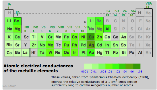
Electrical conductivities of the metallic elements vary over a wide range.
Notice that those of silver and copper (the highest of any metal) are in classes by themselves. Gold and aluminum follow close behind.
Why are metals good heat conductors?
 Everyone knows that touching a metallic surface at room temperature produces a colder sensation than touching a piece of wood or plastic at the same temperature. The very high thermal conductivity of metals allows them to draw heat out of our bodies very efficiently if they are below body temperature. In the same way, a metallic surface that is above body temperature will feel much warmer than one made of some other material. The high thermal conductivity of metals is attributed to vibrational excitations of the fluid-like electrons; this excitation spreads through the crystal far more rapidly than it does in non-metallic solids which depend on vibrational motions of atoms which are much heavier and possess greater inertia.
Appearance: why are metals shiny?


We usually recognize a metal by its “metallic lustre”, which refers to its ability of reflect light. When light falls on a metal, its rapidly changing electromagnetic field induces similar motions in the more loosely-bound electrons near the surface (this could not happen if the electrons were confined to the atomic valence shells.) A vibrating charge is itself an emitter of electromagnetic radiation, so the effect is to cause the metal to re-emit, or reflect, the incident light, producing the shiny appearance. What color is a metal? With the two exceptions of copper and gold, the closely-spaced levels in the bands allow metals to absorb all wavelengths equally well, so most metals are basically black, but this is ordinarily evident only when the metallic particles are so small that the band structure is not established.
The distinctive color of gold is a consequence of Einstein's theory of special relativity acting on the extremely high momentum of the inner-shell electrons, increasing their mass and causing the orbitals to contract. The outer (5d) electrons are less affected, and this gives rise to increased blue-light absorption, resulting in enhanced reflection of yellow and red light.
The thermionic effect: escape of the electron gas
The electrons within the electron fluid have a distribution of velocities very much like that of molecules in a gas. When a metal is heated sufficiently, a fraction of these electrons will acquire sufficient kinetic energy to escape the metal altogether; some of the electrons are essentially “boiled out” of the metal. This thermionic effect, which was first observed by Thomas Edison, was utilized in vacuum tubes which served as the basis of electronics from its beginning around 1910 until semiconductors became dominant in the 1960’s.
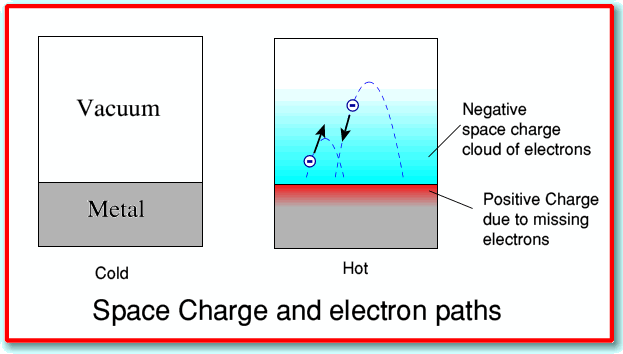
Illustration from a U. of St. Andrews article on Thermionic emission
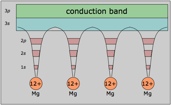
Most metals are made of atoms that have an outer configuration of s2, which we would expect to completely fill the band of MO’s we have described. With the band completely filled and no empty levels above, we would not expect elements such as beryllium to be metallic. What happens is that the empty p orbitals also split into a band. Although the energy of the 2p orbital of an isolated Be atom is about 160 kJ greater than that of the 2s orbital, the bottom part of the 2p band overlaps the upper part of the 2s band, yielding a continuous conduction band that has plenty of unoccupied orbitals. It is only when these bands become filled with 2p electrons that the elements lose their metallic character.
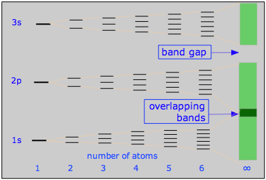 This diagram illustrates the band structure in a 3rd-row metal such as Na or Mg, and how it arises from MO splitting in very small units M2 - M6. The conduction bands for the "infinite" molecule MN are shaded.
In most metals there will be bands derived from the outermost s-, p-, and d atomic levels, leading to a system of bands, some of which will overlap as described above. Where overlap does not occur, the almost continuous energy levels of the bands are separated by a forbidden zone, or band gap. Only the outermost atomic orbitals form bands; the inner orbitals remain localized on the individual atoms and are not involved in bonding.
 In its mathematical development, the band model relies strongly on the way that the free electrons within the metal interact with the ordered regularity of the crystal lattice. The alternative view shown here emphasizes this aspect by showing the inner orbitals as localized to the atomic cores, while the valence electrons are delocalized and belong to the metal as a whole, which in a sense constitutes a huge molecule in its own right.
The band theory of solids provides a clear set of criteria for distinguishing between conductors (metals), insulators and semiconductors. As we have seen, a conductor must posses an upper range of allowed levels that are only partially filled with valence electrons. These levels can be within a single band, or they can be the combination of two overlapping bands. A band structure of this type is known as a conduction band.
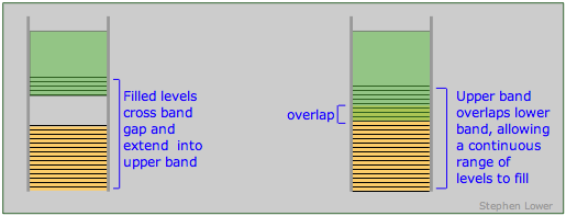
Band arrangements in conductors. Metallic conduction requires the presence of empty levels into which electrons can move as they acquire momentum. This can be achieved when a band is only partially occupied or overlaps an empty band (right), or when the gap between a filled band and an upper empty one is sufficiently small (left) to allow ordinary thermal energy to supply the promotion energy.
Insulators and semiconductors
An insulator is characterized by a large band gap between the highest filled band and an even higher empty band. The band gap is sufficiently great to prevent any significant population of the upper band by thermal excitation of electrons from the lower one. The presence of a very intense electric field may be able to supply the required energy, in which case the insulator undergoes dielectric breakdown. Most molecular crystals are insulators, as are covalent crystals such as diamond.
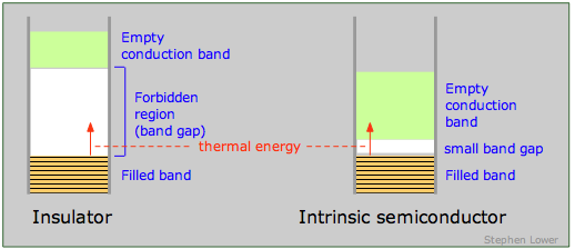
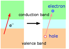
If the band gap is sufficiently small to allow electrons in the filled band below it to jump into the upper empty band by thermal excitation, the solid is known as a semiconductor. In contrast to metals, whose electrical conductivity decreases with temperature (the more intense lattice vibrations interfere with the transfer of momentum by the electron fluid), the conductivity of semiconductors increases with temperature. In many cases the excitation energy can be provided by absorption of light, so most semiconductors are also photoconductors. Examples of semiconducting elements are Se, Te, Bi, Ge, Si, and graphite.
Semiconductor materials have traditionally been totally inorganic, composed mostly of the lighter P-block elements. More recently, organic semiconductors have become an important field of study and development.
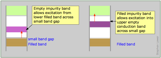
The presence of an impurity in a semiconductor can introduce a new band into the system. If this new band is situated within the forbidden region, it creates a new and smaller band gap that will increase the conductivity. The huge semiconductor industry is based on the ability to tailor the band gap to fit the desired application by introducing an appropriate impurity atom (dopant) into the semiconductor lattice. The dopant elements are normally atoms whose valance shells contain one electron more or less than the atoms of the host crystal.
Thermal properties of semiconductors
 At absolute zero, all of the charge carriers reside in lower of the bands below the small band gap in a semiconductor (that is, in the valence band of the illustration on the left above, or in the impurity band of the one on the right.) At higher temperatures, thermal excitation of the electrons allows an increasing fraction jump across this band gap and populate either the empty impurity band or the conduction band as shown at the right. The effect is the same in either case; the semiconductor becomes more conductive as the temperature is raised. Note that this is just the opposite to the way temperature affects the conductivity of metals.
How N- and P-type materials conduct electricity
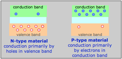 For example, a phosphorus atom introduced as an impurity into a silicon lattice possesses one more valence electron than Si. This electron is delocalized within the impurity band and serves as the charge carrier in what is known as an N-type semiconductor. In a semiconductor of the P-type, the dopant might be arsenic, which has only three valence electrons. This creates what amounts to an electron deficiency or hole in the electron fabric of the crystal, although the solid remains electrically neutral overall. As this vacancy is filled by the electrons from silicon atoms the vacancy hops to another location, so the charge carrier is effectively a positively charged hole, hence the P-type designation.
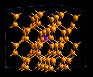
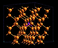
Structure of As (magenta) doped into crystalline Si (yellow.) [source]
Substitution of just one dopant atom into 107 atoms of Si can increase the conductivity by a factor of 100,000.
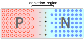 When P- and N-type materials are brought into contact, creating a PN junction. Holes in the P material and electrons in the N material drift toward and neutralize each other, creating a depletion region that is devoid of charge carriers. But the destruction of these carriers leaves immobile positive ions in the N material and negative ions in the P material, giving rise to an interfacial potential difference ("space charge") as dipicted here. As this charge builds up, it acts to resist the further diffusion of electrons and holes, leaving a carrier-free depletion region which acts as a barrier at the junction interface.
A new class of organic PN junctions makes use of mobile positive and negative ions as charge carriers.
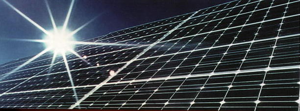
Many of the practical applications of semiconductors depend on the manipulation of this PN junction potential. Among these are certain types of photovoltaic solar cells.
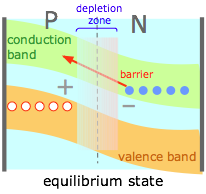 (1) |
The effect of the depletion region is to create a potential energy barrier to the diffusion of electrons from the N into the P material. This is expressed by "bending" the conduction and valence bands as is shown here. (Note that these diagrams are constructed for electrons; the positive charge of the holes causes this barrier to appear inverted on such a diagram.) |
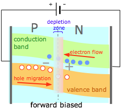 (2) |
If an external potential difference is applied to the junction so as to counteract the space charge, the negative charge on the N side raises the energy of the electrons in the conduction band and of the holes in the valence band, reducing the barrier heights for both (and reducing the width of the depletion zone.) Electrons and holes can now tunnel across this zone. A forward-biased junction allows the PN junction as a whole to behave very much like a conductor. |
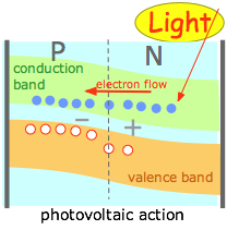 (3) |
Another way of boosting the energy of the charge carriers to overcome the depletion zone barrier is to use a materials that are capable of absorbing light of an appropriate wavelength and which can efficiently couple the energy of the absorbed photons to the charge carriers. This is the basis of the very important photovoltaic or solar cell. There are many other kinds of photovoltaic cells. See this Wikipedia article for more information. |
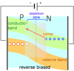 (4) |
If an external potential is applied to a PN junction so as to reinforce the space charges within the two regions, the barrier height and depletion zone width are increased, greatly inhibiting the flow of either kind of carrier into the opposite region. A PN junction thus acts as an electrical diode, allowing current to pass through in only one direction. If an alternating voltage is applied to the diode, it acts as a rectifier, convering ac into interrupted dc. |
 (5) |
See this Wikipedia article for much more on light-emitting diodes. |
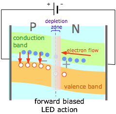
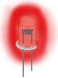 By selecting the right kinds of semiconductor materials, the electrons entering the P side of a forward-biased junction can be made to fall into the holes already present in the valence band (compare this diagram with (1) above.) The energy lost by the electrons (vertical red arrows) is emitted as light, creating a light-emitting diode or LED.